Introduction
Matrix multiplication is among the most foundational of algorithms in scientific computing, used in fields ranging from computational fluid dynamics to artificial intelligence. Naturally, building high-performance implementations is of great concern to engineers. The massive parallelism provided by GPUs has heightened interest in the possibilities of hardware acceleration, leading some firms to develop custom hardware intended solely for matrix operations, such as Google’s TPU. In this post, I will demonstrate a hardware matrix multiplier implementation targeting AMD’s Zynq 7000 SoC.
Credit
This blog post was inspired by Georgia Tech Professor Callie Hao’s ECE 8893 graduate course, Parallel Programming for FPGAs. I use the reference implementation as a starting point for my optimization. The course materials are publicly available on GitHub.
For the sake of consistency, both the reference implementation and my optimized implementation multiply a 

Zynq SoC
AMD’s Zynq 7000 contains an ARM processor that interfaces with a programmable logic device. This SoC is compatible with Pynq, a set of Python libraries that enable programs to interface with custom hardware, akin to how NVIDIA’s CUDA libraries provide a convenient API for GPU kernel developers.
High-Level Synthesis (HLS)
HLS tools, like AMD’s Vitis HLS suite, enable hardware engineers to define algorithms in high-level languages that are translated to RTL implementations. HLS eliminates some of the burden of implementing performance optimizations directly in HDLs.
Accelerator Design
Reference Implementation
The provided implementation contains three main steps:
- Load the operand matrices from system DRAM to local BRAM
- Use a nested loop to compute the matrix product, storing the result in BRAM
- Copy the result matrix from BRAM to DRAM
This approach is sensible, but there are a few major issues with the implementation:
- For very large matrices, it is impractical to copy them fully from system memory to constrained local memory
- The opportunities provided by the FPGA’s concurrency are left untapped; if the dependencies between data are minimal, it is simple to express intent for concurrent execution
- Only one AXI bundle is in use, limiting the memory bandwidth of the kernel
My design remedies these pitfalls, achieving a four times performance increase.
Reference Synthesis Performance Report:
Notice that the reference implementation needs an estimated 3.3M cycles for one matrix multiplication. My optimized implementation only needs 788K cycles, but the speedup comes at a cost: Significantly higher resource usage.
Optimized Implementation
My design offers the following benefits over the reference design:
- My design leverages block matrix multiplication, as outlined in Kastner et al. (141), significantly increasing scalability. Because block multiplication operates on subsets of the larger matrix operands, it is ideal for streaming use cases, enabling my design to scale to larger matrices that might not fit entirely in local memory
- I use a
BLOCK_SIZEof4, meaning that each block multiplication involves amatrix and a
matrix, resulting in a
matrix. For optimal performance,
BLOCK_SIZEshould be a power of 2. The performance of my implementation doubled when I increased theBLOCK_SIZEfrom2to4
- I use a
- The loops in my code are pipelined with a target initiation interval of 1. That is, one iteration of each pipelined loop completes every clock cycle, improving hardware utilization (e.g., memory transfers are not blocked as computation progresses)
- I allocate three AXI bundles for communication, improving kernel throughput. Additionally, using separate AXI bundles enables me to decorate the
CallBlockMatmulloop with theDATAFLOWpragma - The three function calls inside the
CallBlockMatmulloop are part of a dataflow. Dataflows are like pipelines, enabling the loop to iterate as function calls continue - I partition the BRAM buffers, delivering a slight performance improvement. Partitioning enables further data parallelism
- According to AMD’s documentation, the
array_partitionpragma cannot be used with the DRAM buffers, since my design interfaces with host DRAM throughm_axiinterfaces
- According to AMD’s documentation, the
My design provides a starting point for multiple other projects and improvements:
- As I alluded to earlier, my design is well-suited for streaming. I would like to test my code against larger matrices
- Rather than using two sets of doubly-nested loops to transfer data from DRAM to BRAM, it is possible to use one nested loop with some simple branching logic
- My design uses block array partitioning, but others have had success with cyclic partitioning. I would like to explore other partitioning schemes further
Hardware Testing
Vivado Workflow
AMD’s Vivado tool allows hardware engineers to integrate custom IP cores produced by Vitis HLS with other components in their design. Vivado automatically configures the AXI bus infrastructure, enabling seamless communication between the matrix multiplication IP core and the ARM processor.
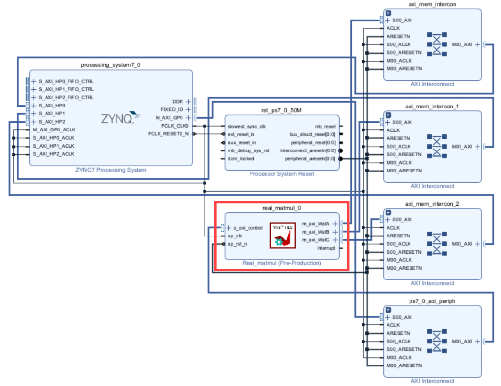
MatA, MatB, and MatC.After generating an HDL wrapper for my design, Vivado synthesizes the HDL and produces a bitstream. The Zynq SoC only needs an automatically-generated hardware handoff file and a bitstream to leverage a new design.
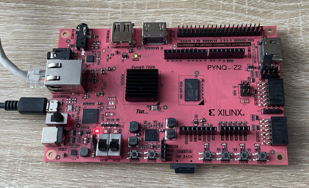
Development Board
I use the Pynq library to flash my design onto the SoC and test it using randomly-initialized Numpy arrays. I recommend the popular TUL PYNQ Z2 development board, which contains GPIO headers compatible with common microcontrollers. After flashing the board’s SD card with TUL’s Linux image, I navigate to its Jupyter interface in my browser. The following Python script validates my design.