Introduction
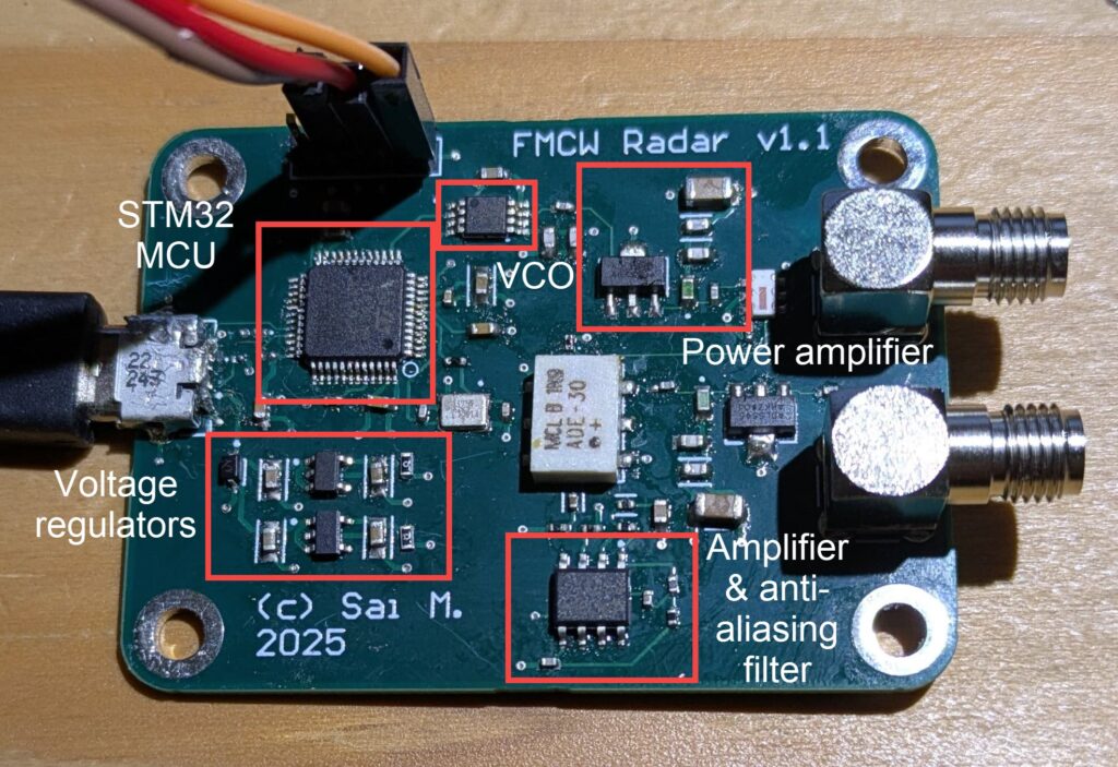
Radar technologies remain essential to critical national security functions. Modern radars dramatically eclipse the capabilities of the first radars deployed in WWII, but the foundational principles of electromagnetic sensing animate all radars deployed over the past eighty years. I developed a low-cost Frequency-Modulated Continuous Wave (FMCW) radar to improve my understanding of radars and practical radio frequency (RF) design.
System Parameters
FMCW radars, unlike traditional pulsed radars, transmit continuously. The radar mixes the transmitted frequency-modulated waveform with the reflected waveform, producing a beat frequency that indicates the distance to an object. Doppler frequency shifts provide velocity information, although my radar design doesn’t (yet) exploit the Doppler effect.
| Parameter | Value |
| Chirp Bandwidth | 100 MHz |
| Ramp Time | 5 ms |
| Maximum Unambiguous Range | 112.5 m |
| Receiver Bandwidth | 15 kHz |
The maximum unambiguous range is determined by the chirp bandwidth, the receiver bandwidth (the design constraint I chose), and the ramp time. Simple hardware, including low-end oscilloscopes and even PC sound cards, can sample data at 30 kHz (15 kHz bandwidth signals, per the Nyquist criterion). The maximum unambiguous range of 112.5 m permitted by my chirp parameters is more than sufficient for my low-power transmitter (18 dBm).
Simple relationships describe how these parameters interact. The round-trip propagation time for electromagnetic radiation launched at an object 112.5 m away is 

Antenna Design
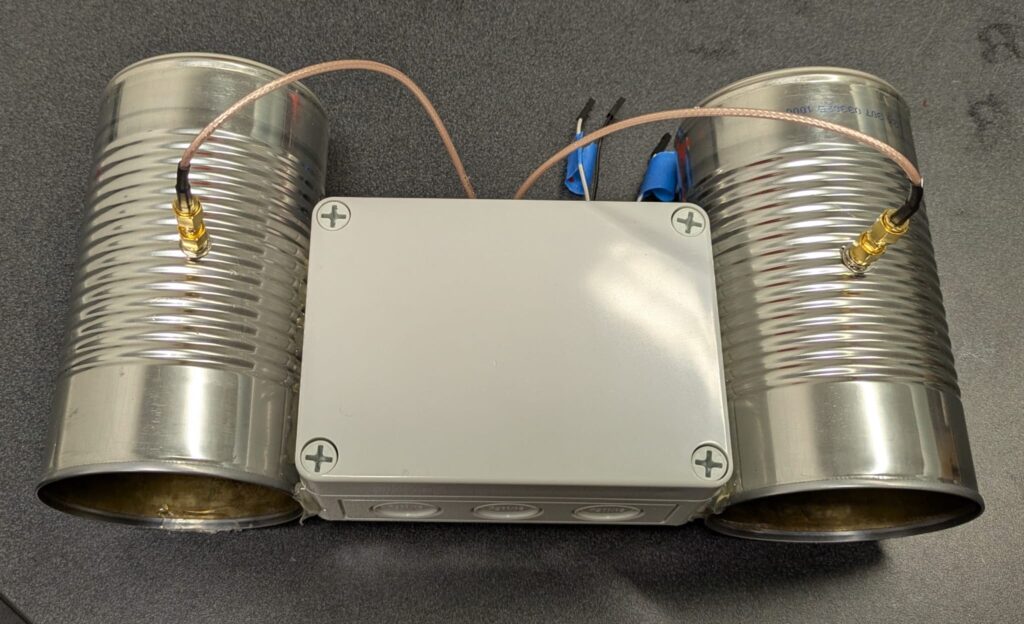
I based my antennas on the Cantenna design popularized by MIT, a quarter-wave monopole resonator inside a circular waveguide. I used a beans can for the waveguide. (The can had corrugated sides, so it cannot be modeled purely as a circular waveguide.)
At 2.4 GHz, the quarter-wave resonator is roughly 3 cm long. Ideally, the length of the monopole would be trimmed until S11 was less than -10 dB across 2370-2470 MHz, but I didn’t have access to a VNA. The antenna was positioned one-quarter of a wavelength from the back wall of the waveguide. Note that the wavelength of the signal inside the waveguide differs from the free space wavelength.
The gain of the antenna can be estimated using the following relation. This is critical for applying the radar equation. Gain is normally measured in decibels relative to an isotropic radiator.


Notably, the Cantennas have a significant -3 dB beamwidth. Radars typically use antennas with narrower beamwidths.

Radiation will only propagate above the TE11 cutoff frequency, which is handily satisfied.

Receiver Modeling
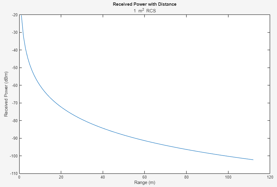
With my antennas selected, I turned my attention to modeling the receiver. The radar equation determines the amount of power received by the radar for an object a given distance away. The radar cross section (RCS) 


Microstrip Transmission Line Design
Like any RF design, care must be taken to ensure low-loss signal transmission. RF engineers achieve a particular characteristic impedance for a planar transmission line by varying the trace width and the distance between the microstrip line and the ground plane, affecting the inductance and capacitance per unit length of the line.
JLCPCB provides a set of four-layer board stackup options, so the only parameter I could vary was the trace width. I wrote a MATLAB script using Hammerstad’s formulas to solve for the trace width that achieved 50 Ω.
Warning: Unable to solve symbolically. Returning a numeric solution using vpasolve.
> In sym/solve (line 313)
In Microstrip_Line_Solver (line 16)
Width: 0.187268 mm (7.372736 mil)
Wavelength in TX Line: 0.067843 m
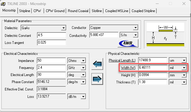
The TXLINE tool in the AWR suite provides a similar result, but it is more accurate, since it incorporates frequency-dependent behavior. Calculators like TXLINE appear to render manual calculations obsolete; however, I always like to validate the results of third-party tools. The MATLAB calculation also provides other useful information, like the wavelength of the signal in the transmission line. Transmission line effects typically only need to be considered when the length of the line 

AWR can provide more insight into the behavior of transmission lines across the frequencies of interest. I modeled my substrate and a quarter-wavelength run of my transmission line in a schematic file.
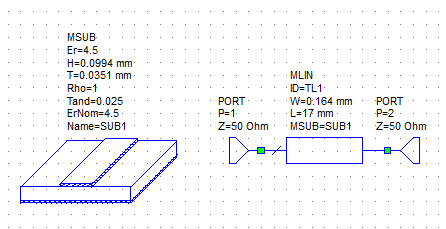
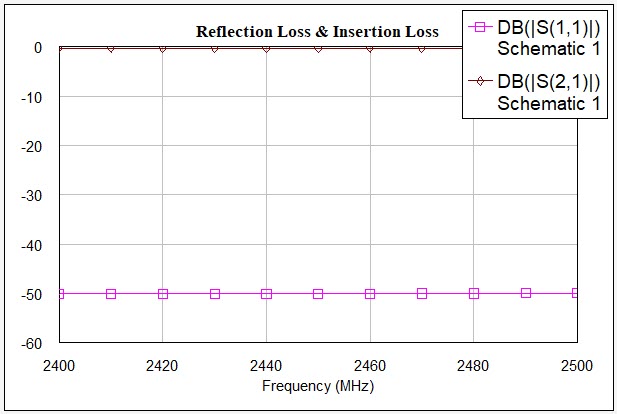
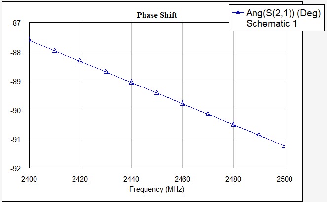
I plotted S11 (reflection loss) and S21 (insertion loss) from 2.4 to 2.5 GHz, demonstrating the transmission line’s excellent performance. The phase shift of the quarter-wavelength line is around 90°, as we expect. (Quarter-wavelength lines are useful for narrowband impedance matching.)
As useful as closed-form solvers are, they don’t always reveal issues in board layouts. Microstrip calculations expect free space above the transmission line. I mistakenly routed portions of my line under components, breaking this assumption. The EM simulation capabilities in AWR or a dedicated tool like CST (the subject of another project) help catch such mistakes.
Baseband Analog Circuitry
The baseband circuitry follows the mixer and has two responsibilities: (1) Amplifying the uV-level signal from the mixer output and (2) providing a low-pass filter response to avoid aliasing. Two LT6230 op-amps were used (the LT6231 contains two LT6230 devices in one package).
Amplifier
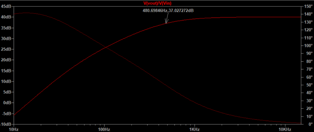
The baseband amplifier magnifies the small-signal AC variation from the mixer output and adds a DC offset (ideally centered) between the 3.3V and ground rails. I began my design of the baseband amplifier by considering the AC RMS output voltage from the mixer as a function of distance. Because the system is normalized to 50 Ω, I can easily calculate the AC RMS voltage using the power output from the mixer: 

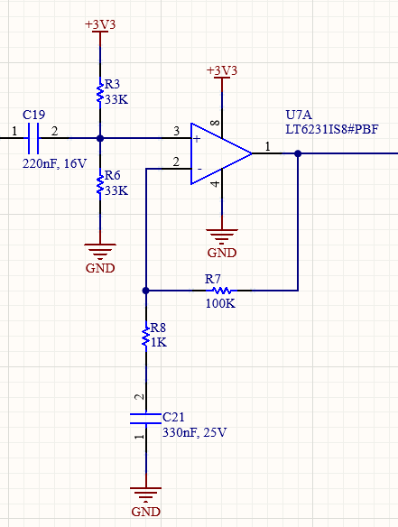
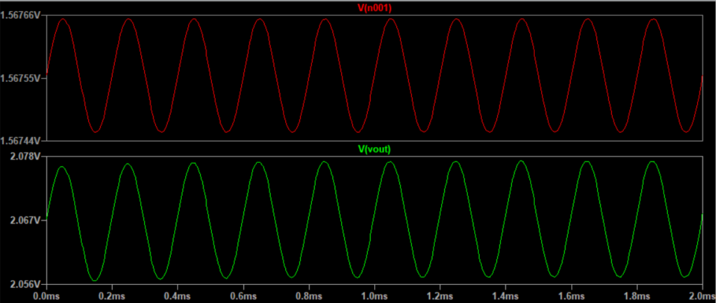
I chose 33 kΩ biasing resistors to produce a biasing current of approximately 50 uA. Notably, the LT6231 is a non-ideal op-amp, and both the inverting and non-inverting inputs draw 5 uA, according to my SPICE simulations. This input current sets the DC offset of the output terminal 0.5 V above the biasing of the non-inverting input. The size of the mismatch between the expected and actual output DC bias voltage depends on the value of R7, limiting the maximum gain of the amplifier. (If R7 is too large, the output voltage will have a large DC offset, causing the op-amp to saturate.) I updated my design so that R7 and R8 produce a non-inverting gain of 101, but I gathered the test results presented here using a gain of 301. The 3 V offset that came with a gain of 301 wasn’t especially problematic for my testing because an unloaded LT6231 can swing, in the worst case, within 70 mV of its upper 3.3 V rail (see Page 5 of the LT6230/1/2 datasheet). The ADC has a negligible loading effect on the op-amp, and the op-amp presents very low impedance to the ADC.
C21 influences the location of the high-pass pole by shorting R8. The high-pass pole is located at 

Anti-Aliasing
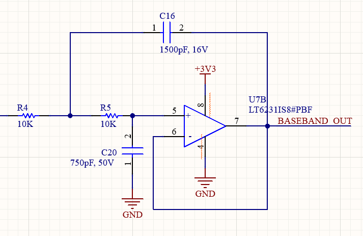
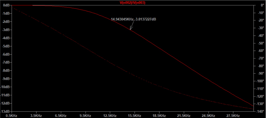
The anti-aliasing filter enforces the 15 kHz receiver bandwidth. I implemented a second-order Butterworth filter using the Sallen-Key topology. The design relations for the Butterworth Sallen-Key topology are well-documented in this TI application note. I fixed the values of R4 and R5 and calculated C16 and C20 to achieve a 15 kHz cutoff frequency.
Noise Analysis
Noise analysis helps radar designers track the degradation of SNR from input to output through the receiver chain. In this design, the antenna is fed to a PA and mixer before the baseband circuitry. This noise analysis excludes the baseband op-amp filters and the MCU ADC because they operate at low frequencies and contribute relatively little to the noise floor compared to the mixer and PA.
Applying Friis’ formula requires the gain and noise factor (linear-scale/non-dB noise floor) of the mixer and PA.
| Component | Gain | Noise Factor | Conditions |
| ADL5545 (PA) | 125.89 (~21 dB) | 2.51 (4 dB) | 2.4 GHz |
| ADE-30+ (Mixer) | 0.21 (-6.79 dB) | 4.78 (6.79 dB) | RF = 2450 MHz LO = 2480 MHz LO Power = +7 dBm |
With this information, we can calculate the noise figure.


Because of the large PA gain, the mixer has effectively no contribution to the noise figure of the receiver chain. The PA’s large noise figure dominates. This is why receivers typically use LNAs instead of PAs.
The mixer also has a local oscillator (LO) input, which is driven by the VCO through a coupler and attenuator. LO phase noise can mix with blockers through reciprocal mixing, producing interference in the baseband that masks target detections. We can calculate the threshold at which blocker power becomes comparable to the receiver chain noise floor.
The minimum noise power in a receiver with a 14.5 kHz bandwidth is -132.4 dBm (


| Frequency Offset | LO Phase Noise | Blocker Power Threshold |
| 0.1 MHz | -93 dBc/Hz |  (The  term cancels) term cancels) |
| 1 MHz | -117 dBc/Hz |  |
| 10 MHz | -130 dBc/Hz |  |
Radar designers can increase the blocker power threshold (and thus reduce the sensitivity to interferers in the environment) by using a phase-locked loop as the LO, reducing the phase noise.
Software Design
Firmware
An FMCW radar must synchronize transmission and reception to properly measure the beat frequency. The STM32 family of microcontrollers was chosen for its rich set of hardware timing peripherals and support for DMA, transferring the responsibility of synchronization to hardware. In retrospect, however, the 12-bit ADC provided an insufficient 0.8 mV/LSB resolution.
A common timer drives the ADC (RX stage) and DAC (transmit stage). The DAC accesses a pre-calculated lookup table to sweep the VCO. The ADC uses half transfer and full transfer callbacks to access the sampled values. The firmware currently implements a 51.2 kHz sampling rate (capable of sampling frequencies up to 25.6 kHz without aliasing), but even a 25.6 kHz sampling rate works reasonably because the radar is unlikely to operate well at far distances where high beat frequencies are produced.
During the assembly process, the USB connector broke off the board (I forgot to solder the mechanical attachment through-hole pins). To access the sampled data for post-processing, I developed a PowerShell script that used the OpenOCD debugger to interrupt the firmware when the ADC buffer was fully populated and write the buffer contents to a hex file. I developed the firmware using STMicroelectronics’ Eclipse-based STM32CubeIDE, which lacked the ability to write buffer contents to a file in the debugger.
VCO Sweep
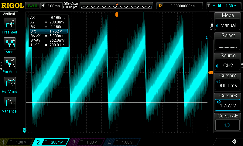
My FMCW radar uses a linear frequency sweep, also known as a chirp. However, the output frequency of a VCO doesn’t vary linearly with the applied tuning voltage. I received assistance from an AI agent to develop a Python script that modeled the tuning voltage curve and generated a lookup table that the MCU could sweep to produce a chirp.
Results
Initially, I developed my board using a baseband amplifier gain of 301, placing the DC offset at roughly 3 V. As mentioned earlier, this would normally be a poor use of the ADC’s dynamic range, but the received signal was so small that even after amplification, the sum of the DC offset and the voltage swing remained well below the op-amp’s rails.
My initial firmware sampled the ADC/DAC at 25.6 kHz, which would alias signal components above 12.8 kHz. I was testing in a small room (5-10 m long), so I didn’t expect to see beat frequencies anywhere near the Nyquist cutoff. I captured 10 milliseconds of the baseband signal (256 samples at 25.6 kHz) using the debugger script.

Interestingly, I observed a strong peak just after 5 milliseconds, when the transmit ramp completed. (The ADC and DAC are clocked together.) There appears to be strong coupling between the transmit and receive antennas, producing spurious peaks.
The system gain also appears to be less than calculated. This is likely due to the abrupt transition between the SMA connector and the narrower impedance-controlled trace on the board, creating reflections that dissipate considerably the power at the mixer’s input.
We can observe an FFT of the capture to determine the beat frequency. The signal appears to have broadband noise, reinforcing my belief that poor isolation is to blame.

Nonetheless, a peak appears at 6.8 kHz, roughly 10 dB (in voltage units) above the noise floor. (I estimated the noise floor by taking the median of the FFT in linear units, then converting to dB.) With my sweep parameters, that comes out to 51 meters.
Photos